- +86 186 0306 4711
- Jianfeng@hongyuanlai.com

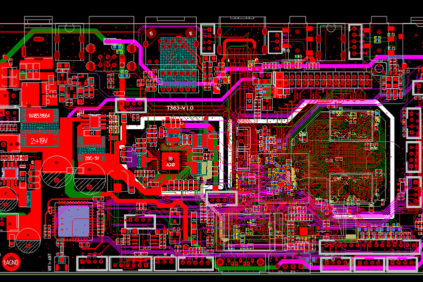
The process of PCB board design always starts with a schematic. A schematic or circuit diagram conveys the electrical connections between different electronic components such as integrated circuits (ICs) and discrete components. To provide this PCB design service, we use specialized CAD software, such as Altium Designer, to define the modules and design the connections between the different components.
Once the PCB design layout is approved for production, we export it to a format supported by the manufacturer. We prepare a Bill of Materials (BOM) and Gerber file that describes the design requirements for each image of the board. Manufacturers use this documentation as a reference for board fabrication and PCB assembly.
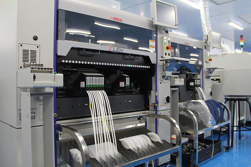
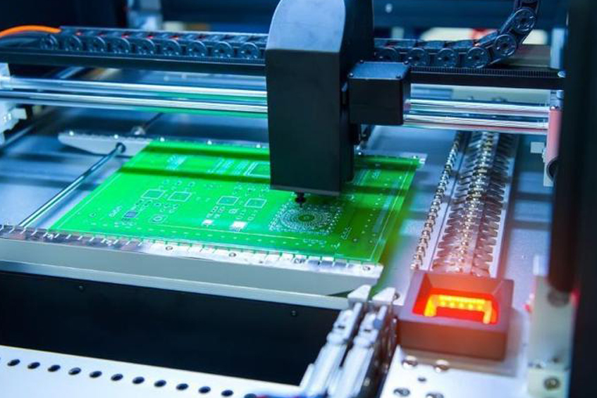
All incoming materials are verified and quality issues are addressed prior to the start of SMT assembly, after which the SMT placement process is completed using automated SMT machines.
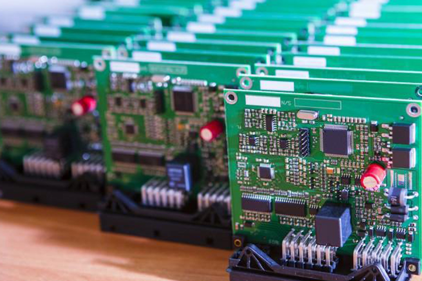
Testing is critical to both our PCB layout design services and the manufacturing phase. We provide manufacturers with the data and software needed to perform resistance and impedance testing. After prototyping is complete, we perform the tests in-house.
After prototype validation, we prepare the documentation for volume production and assist the customer throughout the manufacturing process. We arrange special software, hardware and test programs. Using them, the manufacturer can test each PCB at the factory.

Upon completion of the project, we create a complete documentation package that includes BOM and Gerber files, 3D models and technical manuals. In addition, we offer a warranty period for our PCB design services. During this period, we fix bugs and provide other technical support that is covered by the warranty.